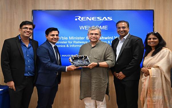
Union Minister for Electronics and Information Technology Ashwini Vaishnaw on Tuesday inaugurated India’s first 3-nanometre (3nm) chip design centres in Noida and Bengaluru, marking a key milestone in the country’s push towards advanced semiconductor innovation. The centres have been set up by Renesas Electronics India Private Limited and are poised to place India among a select group of nations working at the cutting edge of chip technology.
Vaishnaw said, “Designing at 3nm is truly next-generation. We’ve done 7nm and 5nm earlier, but this marks a new frontier.” He added that the launch reaffirms India’s growing presence in the global semiconductor space and reflects increasing industry confidence, witnessed at global platforms such as the World Economic Forum in Davos.
The new centres are part of a broader strategy by the government to build a robust semiconductor ecosystem, spanning design, fabrication, ATMP (Assembly, Testing, Marking, and Packaging), and the supply of associated equipment, chemicals, and gases. The government has also been focusing on nurturing a skilled workforce to meet the growing demand in the semiconductor industry.
Vaishnaw also announced the launch of a new semiconductor learning kit designed to strengthen practical hardware skills among engineering students. Over 270 academic institutions, which have already received access to advanced EDA (Electronic Design Automation) software tools through the India Semiconductor Mission, will also receive these hands-on kits. “This integration of software and hardware learning will create truly industry-ready engineers. We are not just building infrastructure but investing in long-term talent development,” he said, lauding the efforts of CDAC and the ISM team for their efficient execution.
Renesas Electronics CEO and Managing Director Hidetoshi Shibata, who was present at the event, described India as a strategic cornerstone for the company. He said Renesas is expanding its end-to-end semiconductor capabilities in India, from architecture to testing, while actively supporting over 250 academic institutions and a range of startups through government-backed initiatives such as the India Semiconductor Mission and the Production Linked Incentive (PLI) scheme. He also underscored the importance of Indo-Japan collaboration in redefining the global semiconductor lifecycle.