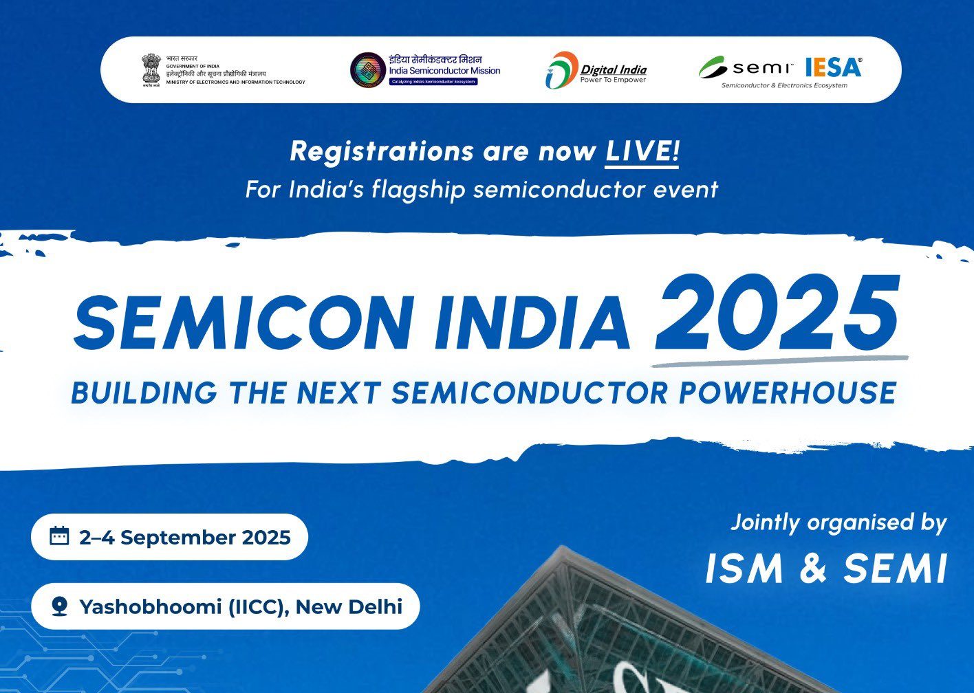
The fourth edition of Semicon India 2025, scheduled for September 2–4 at Yashobhoomi, previously known as India International Convention and Expo Centre – IICC, New Delhi, will see the largest-ever global participation, the Ministry of Electronics and Information Technology (MeitY) announced on Friday.
Jointly organised by the India Semiconductor Mission (ISM) and SEMI, the event aims to showcase India’s expanding capabilities across the microelectronics and semiconductor value chain. This year’s theme is ‘Building the Next Semiconductor Powerhouse’.
According to the ministry, over 300 companies from 18 countries will exhibit at Semicon India 2025 — the highest to date. The event will, for the first time, feature four international pavilions from Japan, South Korea, Singapore, and Malaysia. Eight country roundtables are also planned to promote bilateral partnerships between India and key semiconductor markets.
In line with India’s push to strengthen its talent pipeline, the event will include dedicated skilling and workforce development programmes. Students and engineers will have access to training, upskilling sessions, and career counselling. A dedicated Semiconductor Design Startup Pavilion will highlight innovation-driven chip design firms, while the number of State Government Pavilions has risen to nine from six in the last edition.
The three-day conference will bring together global CXOs, technology leaders, and policy experts to share insights on manufacturing trends, supply chain strategies, and emerging technologies.
The Centre has been working to position India as a trusted semiconductor hub, supported by the Semicon India programme — a ₹76,000-crore initiative to build a robust domestic semiconductor and display manufacturing ecosystem. The government recently revised the programme to keep pace with aggressive incentives offered by other countries and the limited number of companies with advanced node technologies.
In a related development, the Union Cabinet has approved India’s sixth semiconductor manufacturing unit, which will come up near Jewar Airport in Uttar Pradesh through a joint venture between the HCL Group and Taiwan’s Foxconn. The facility, with a capacity of 20,000 wafers per month, is expected to produce 36 million chips monthly and create employment for around 2,000 people.
Meanwhile, work is underway on the other five approved units, one of which is expected to be inaugurated later this year.
To further boost the sector, the government recently amended Special Economic Zone (SEZ) rules to address the unique requirements of semiconductor and electronics component manufacturing. Given the capital-intensive nature and longer gestation periods of these industries, the changes are intended to attract pioneering investments and strengthen India’s position in the global semiconductor landscape.