


India on Friday marked a significant step towards technological self-reliance in advanced electronics with the launch of indigenously developed Silicon Photonics solutions at Indian Institute of Technology Madras (IIT-Madras) in Chennai.
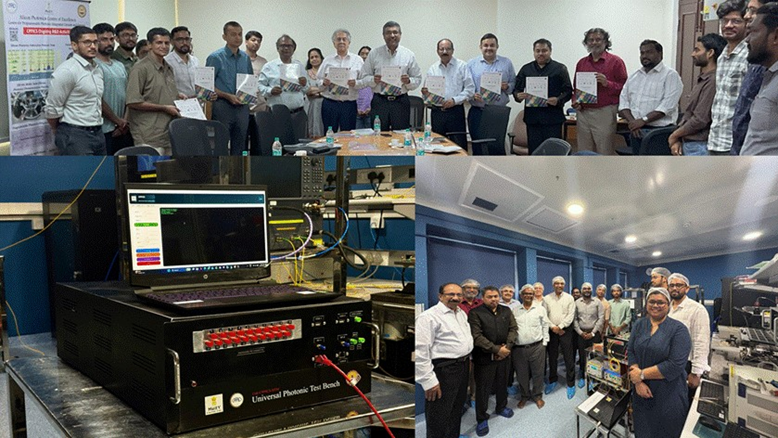
The launch, led by S. Krishnan, Secretary at the Ministry of Electronics and Information Technology (MeitY), introduced two key innovations: a Silicon Photonics Process Design Kit (PDK) and a Universal Programmable Photonic Integrated Circuit (PPIC) Test Engine. Both technologies have been developed at the MeitY-supported Centre of Excellence for Compound Photonics and Photonic Integrated Circuits Systems (CoE-CPPICS) at IIT Madras.
The Ministry of Electronics & IT described the development as a major milestone in India’s journey towards “technology sovereignty” in Silicon Photonics, a cutting-edge field that integrates optical and electronic components on a single chip. The solutions are expected to function as a shared national facility, supporting research and development efforts across academia, industry, startups, and defence organisations.
The newly launched PDK includes more than 50 verified components, providing a comprehensive design ecosystem for building advanced photonic integrated circuits. Meanwhile, the PPIC Test Engine offers a state-of-the-art automated platform for testing and characterising photonic and optoelectronic modules across a range of applications.
Speaking at the event, Krishnan said India’s capabilities in Silicon Photonics are now approaching global benchmarks and stressed the need to complement this progress with the establishment of fabrication infrastructure under the India Semiconductor Mission.
Amitesh Sinha, Additional Secretary at MeitY and CEO of the India Semiconductor Mission, highlighted that the technology has applications in both classical and emerging quantum domains. He noted that further development could be supported under the proposed ISM 2.0 initiative, particularly in the research and development vertical.
The next phase of the project, also announced during the event, will enable multi-project wafer (MPW) fabrication runs starting in the third quarter of the current financial year. This phase will provide integrated capabilities for fabrication, testing, packaging, and module characterisation.
Developed under a Product Research, Development and Manufacturing (PRDM) model, the initiative leverages CMOS-compatible Silicon Photonics technology. It is supported by global and domestic partners, including SilTerra Malaysia as the foundry partner and izmo Microsystems, Bengaluru, for photonic IC packaging.


